Yet Another
Modifying a USB Sound FOB
For Allstar

Click on any image in this document to view larger
Introduction
This is just yet another USB sound FOB modification solution. There are several variations by other authors out on the web and there are many variations of the physical sound FOBS that you can purchase. My goal was to make the modification of the FOB itself as painless as possible. I don't like the idea of removing components or modifying the board as these boards are cheap and even a very careful person can easily damage the boards. I bought ten of these boards for $24 in November, 2014 on Ebay.
Skip ahead to April 2016 and the boards originally listed are no longer available. Also finding unpotted boards that can be modified is getting difficult. The following link is an unpotted board but because the vendor code is different it will only work in the newer code release for the RPi2/3 - see 1.02beta in the download section. You must run the 1.02 version in the beta mode. It will also be supported in all future releases. Future releases will also include another method of obtaining PTT and COS using a USB to serial adapter eliminating the need to modify the sound FOB. Although this howto gives a good description of modifying the FOB you should also review the Simple USB Sound FOB mod link for an easier method.
Here are a couple of FOB sources that at least as of Summer 2016 can be modified.
- https://www.amazon.com/gp/product/B001MSS6CS/ref=oh_aui_detailpage_o03_s01?ie=UTF8&psc=1
- http://www.newegg.com/Product/Product.aspx?Item=N82E16812186035&cm_re=syba_usb-_-12-186-035-_-Product
A note about FOBS
As of the beginning of 2016 it has become increasingly hard to find sound FOBS without potted electronics that allow the below modifications. The above link while not the only possible choice has not shown up potted and it is a smaller footprint FOB allowing for use in a tighter physical installation. In the summer of 2016 we will be announcing a very inexpensive alternative way to derive COS and PTT for multiple nodes using one USB port. The would negate the need to modify the FOBS and any compatible type could be used.
Modification
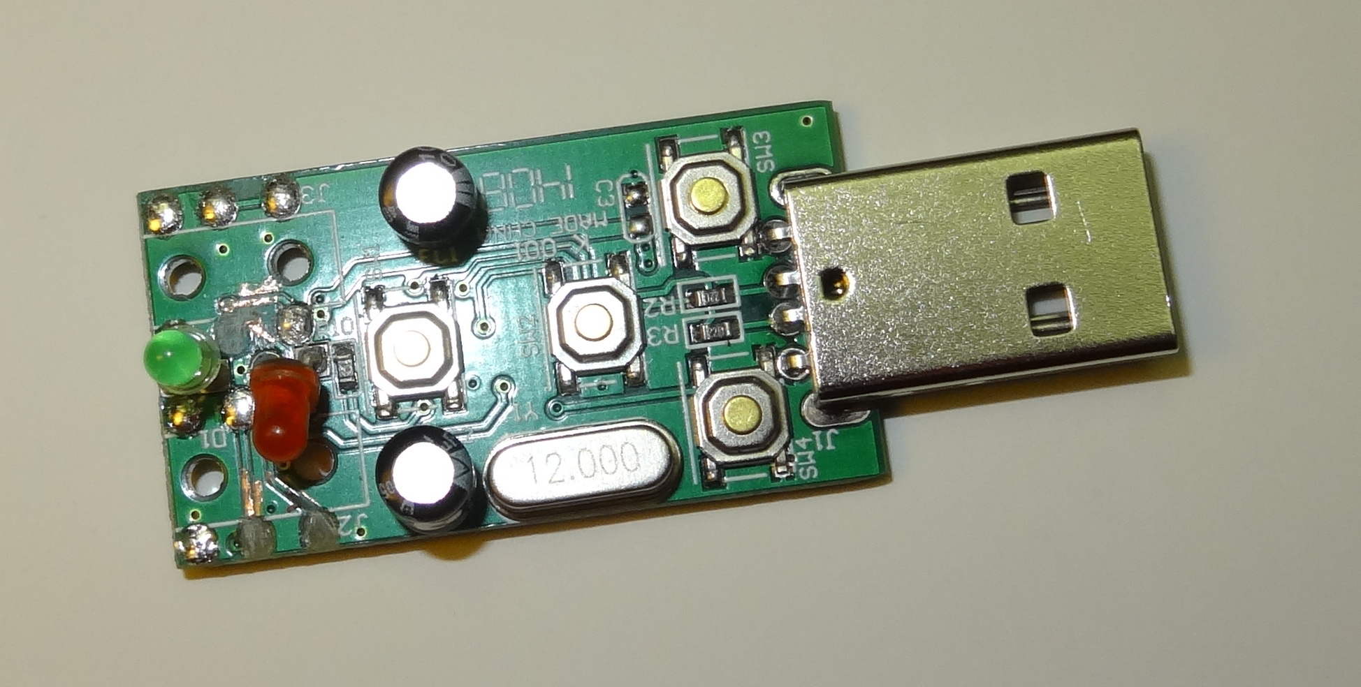
This FOB comes apart very easily. In fact so easily that if you used it the way it was intended it could fall apart in normal use but for the modification that is a good thing. Here are some views of the board removed from the case -


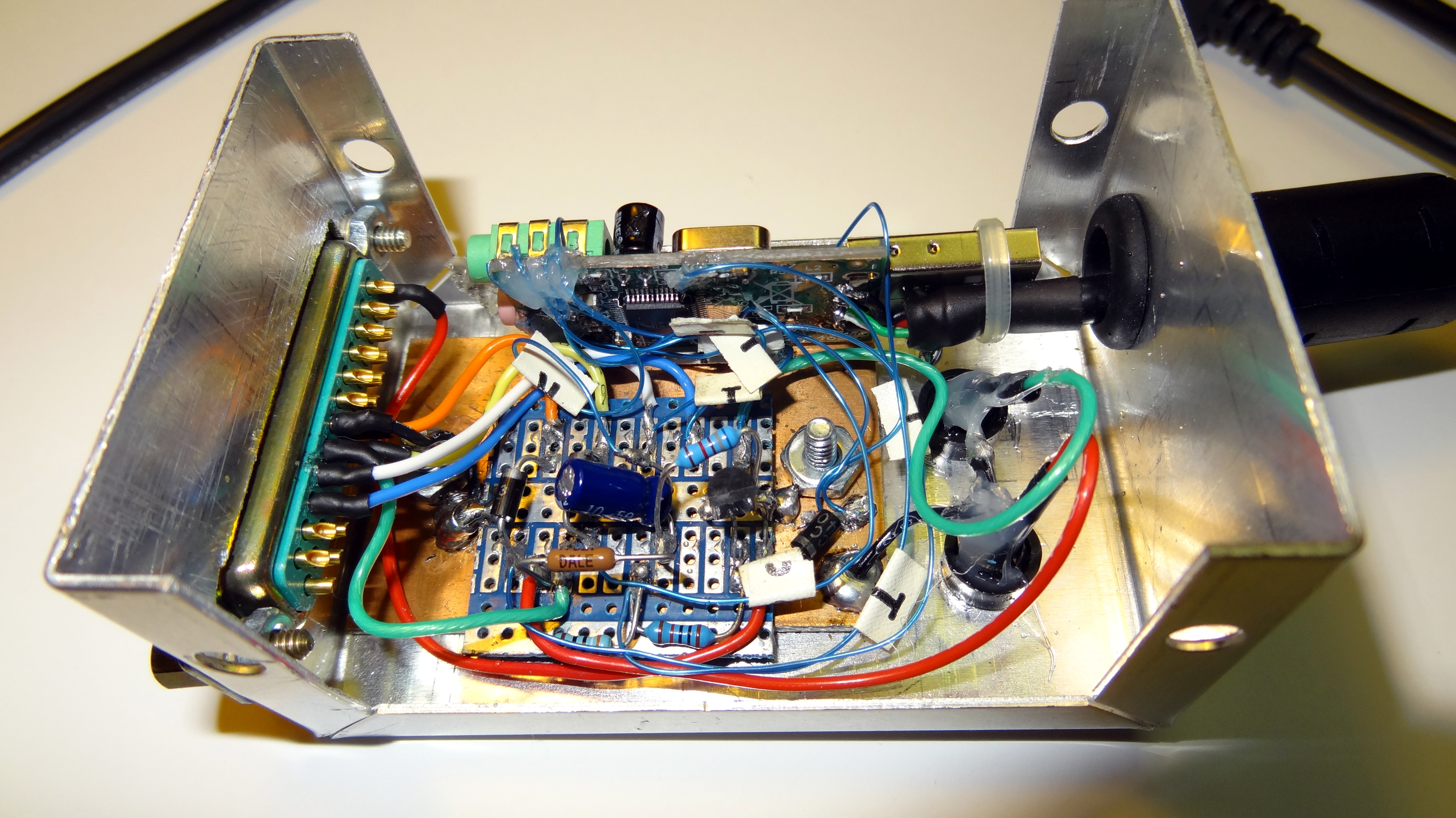
The only modification to the FOB was the soldering of wires to key locations and the cutting of one lead to the on-board green LED. This LED was relocated to the outside box. It is important to use small wire, a small soldering iron, and magnification to perform these modifications. I used #30 wire wrap wire. Do you remember the wire wrap days? If not you are probably a lot younger than I am. Cut and pre-tin the leads and use solder sparingly. There are two connections directly to pins on the CM108 and fortunately it is end pins which are easy to get to. Using the small wire it is very easy to quickly tack the leads on. If you buy a lot of 10 as I did and each board is less than $2.50 then you can afford to sacrifice one for experimentation. If the experiment works then you have not destroyed a board if not it certainly isn't a big loss. Here is a photo my "sacrifice" board. I was following directions on some of the other modifications links below which tell you to remove components and make other modifications to the board. I found none of them to be necessary and the less you do to the board the better. You can clearly see the pads lifted where the audio jacks were removed. I thought I was being careful cutting the connectors out and this was the result. You can see where the pads lifted around the removed audio connector at the bottom right. Not a pretty picture.
So here are photos showing the points where wires were added to a virgin board. Refer to the schematic diagram which details locations and pin numbers.
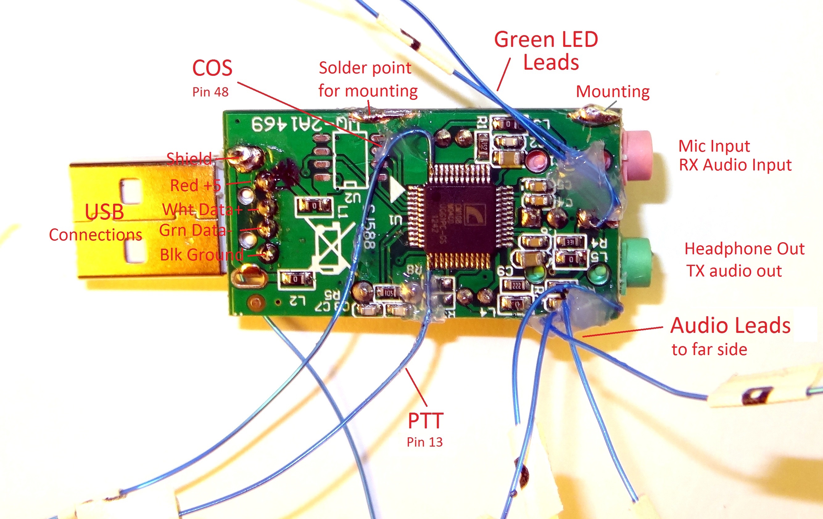
Notice the large white arrow pointing at the CM108 chip in the left photo. This is pin one of the chip and the numbers go counter-clockwise. There are twelve pins per side for a total of 48. The wire connected to pin 13, bottom left of the chip is the PTT connection. The wire connected to the top row, left, pin 48, is the COS connection. The COS connection could also be made to the volume down push button on the other side if you prefer. Other connections shown are the two leads connected to the underside of the green LED and the audio leads coming from the other side of the board.
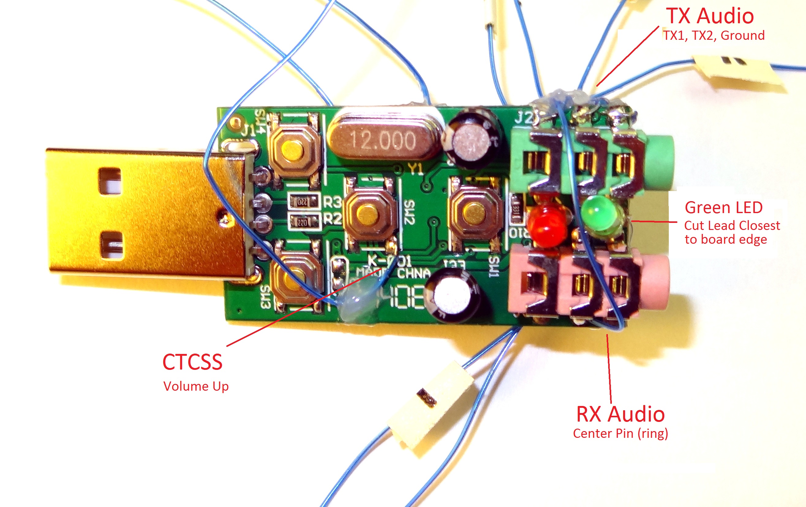
The right photo of the top side of the board shows the CTCSS connection to the Volume UP push button and three connections to the green audio out (TX) jack. Ground (sleeve) at far right, TX1 (ring) center, and TX2 (tip) at left. On the red audio in jack there is one connection to the center (ring) of the connector. The green LED lead closest to the outside of the board is cut to disable this LED. Another green LED is placed on the outside case. Because the leads are small and subject to handling failure I secured them to the board with some clear silicone sealant for protection. All of the leads were labeled so no mixup could occure when connecting them later. No other modifications were made to the board.
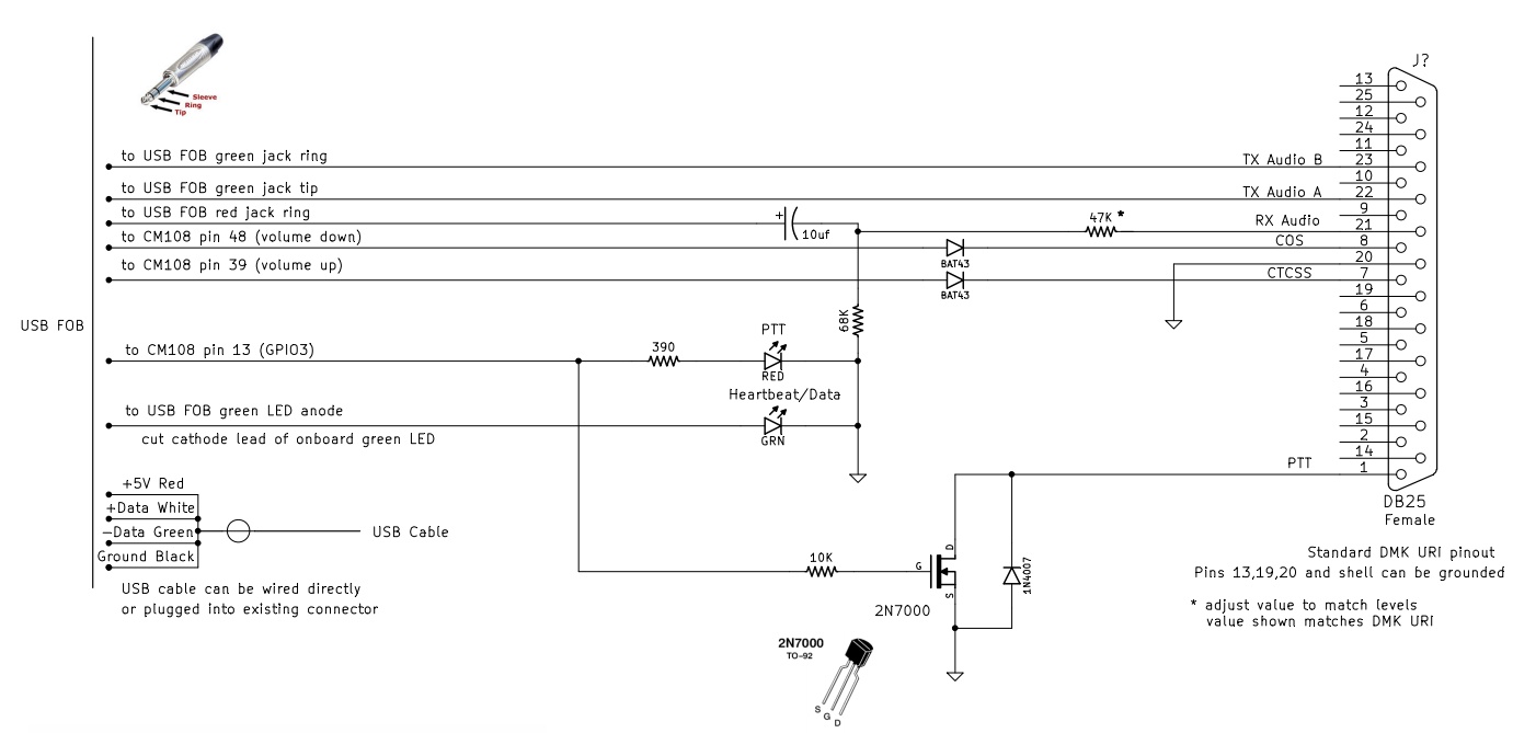
The schematic shows the interface circuitry required between the USB FOB and the 25 pin 'D' connector which is wired with the standard DMK-URI pin-out for the necessary pins. Because the board was not modified there can be bias voltage on the microphone input lead so a 10uf electrolytic is used to block the DC. The resistive divider network values were selected to make the levels equal to a DMK-URI with the same radio. Depending on your input levels you may need to change the values. One circuit used a 100K pot in place of the divider which would work fine but I prefer not to use a pot which being a mechanical device could be a problem in the future. As you will see in the following photos a USB cable was cut and the leads were soldered directly to the existing connection points of the FOB USB connector. Again this is optional and the original connector does not need to be removed. If you prefer you could use a standard extension type cable to connect to the FOB's USB connector. If you do solder wires directly to the pins note that the polarity of the data lines, and ground and 5 volt points are important.
Most other designs use a transistor for the PTT switching but I choose to use a FET. The 2n7000 is often used in amateur designs for PTT control. It has a high (60V) voltage rating and should handle most anything you throw at it. I always put a diode from the PTT to ground for spike prevention. It is probably not needed in most cases but it is cheap insurance. The COS and CTCSS diodes are Schottky but in a pinch you can use a standard diode. Just be aware it could cause problems if levels are on the hairy edge so if you do use a standard diode and you have COS or CTCSS switching problems that might be the cause.
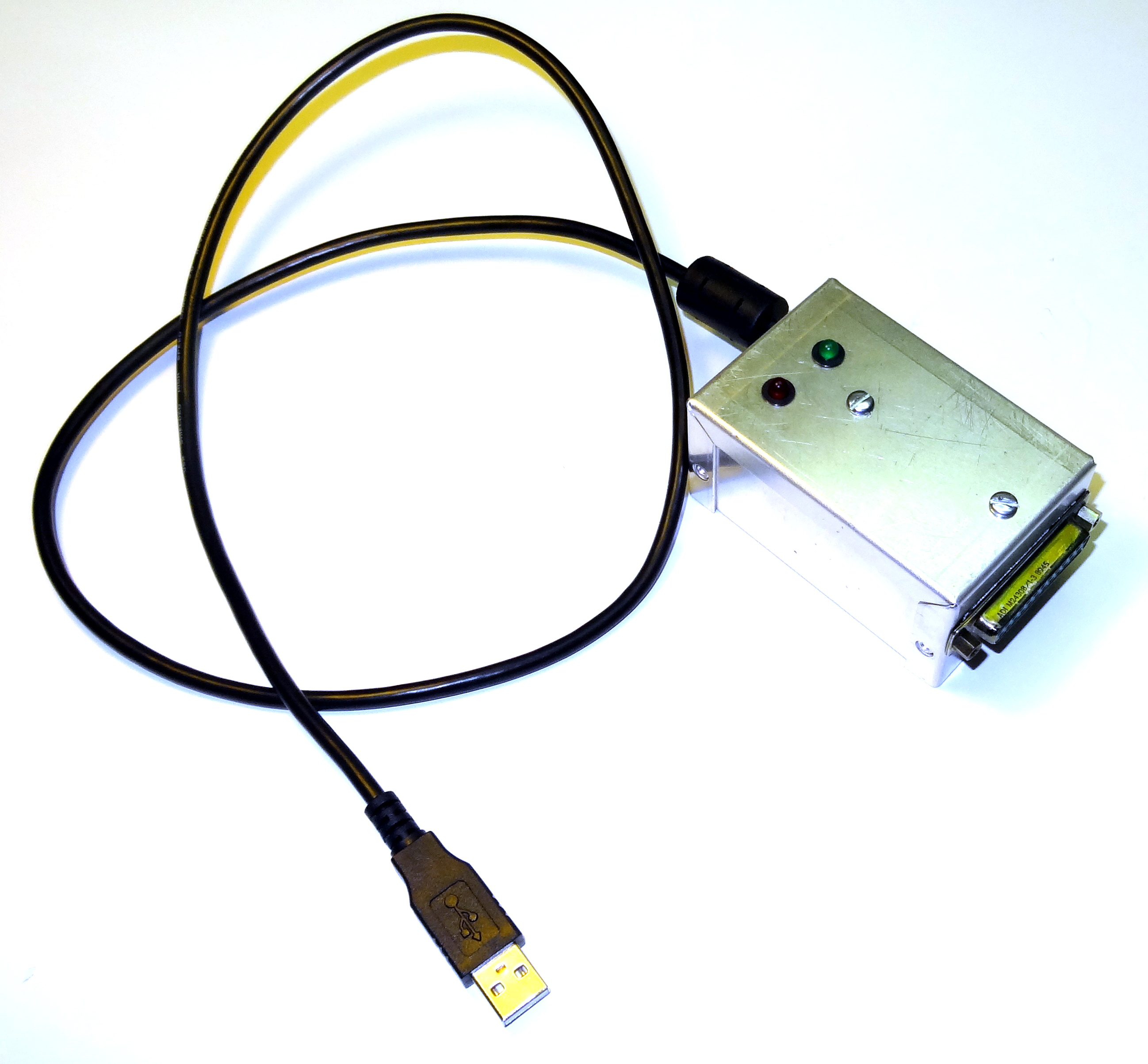
I selected a small Bud box to house the FOB and additional circuity. The small circuit board mounted in the center of the chassis is used for the needed circuitry and connections between the small wires from the USB FOB and those going to the DB25 connector. It is solder mounted to a piece of copper board that is bolted to the chassis. The USB FOB is edge soldered to the copper board. The USB lead enters from the right and is wire tied to the USB connector on the FOB as you can see in the following photo. I cut the end off one of the many old USB cables I have around and it conveniently had a ferrite attached which you can see just outside of the chassis. The four USB leads are soldered directly to the bottom side of the FOB's USB connector pins. The shield is soldered to the FOB's USB shell connection point. Another option is to use the USB chassis mount adapter cable listed below from Adafruit. Keep in mind that the box shown is a prototype and many experimental changes were made along the way so it is not as neat as it could be but it works well.
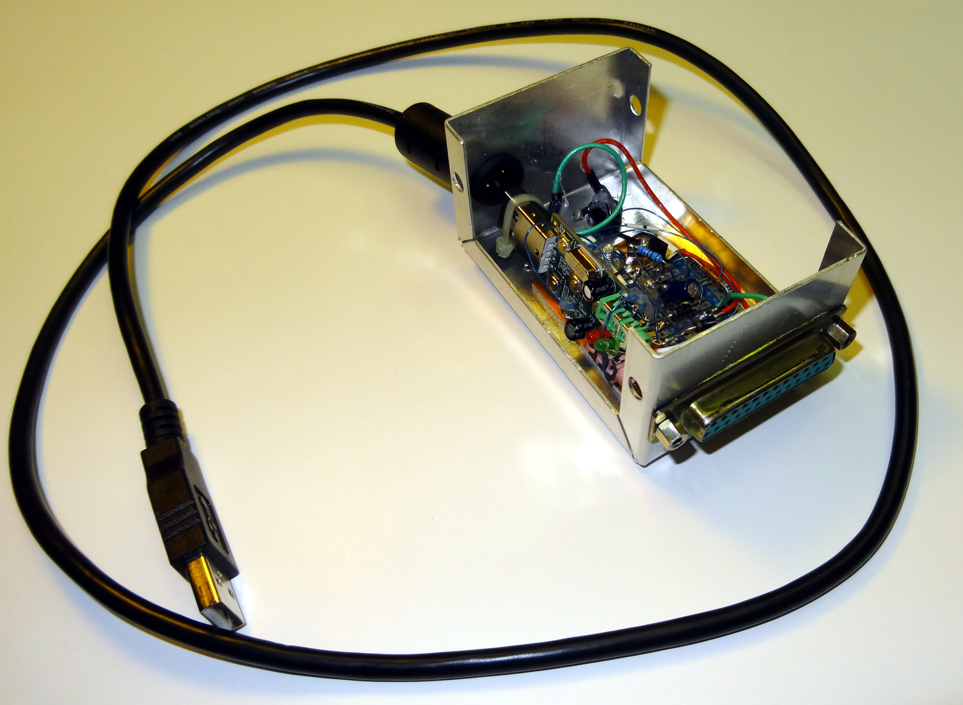
Feel free to use your imagination in how the project is housed. There are many different boxes both metal and plastic that could be used. You also might chose to use a different connector for the radio interface such as a DB9 or maybe no connector at all with just a wire to the radio connector at the other end. I used a DB25 because it makes it fully compatible with the DMK-URI's that I own. That's the fun of a project like this, everyone will approach it a little differently but electrically the end result will be the same.
Final Comments
This modification is probably not for the beginner or one who does not have reasonable eyesight or hand control. On the other hand if you have the confidence to try it the extremely low cost of the boards would mean that you have little to lose other than the time involved. So give it a try and hopefully you will be able to enjoy a very inexpensive Allstar audio interface.
Links
Below are links to data and other methods that were used to modify the FOB's. Note that many of the modification sites are very dated but they are presented for reference. You could also google something like "usb fob modification" for more information.
- CM108 Data Sheet
- 2N7000 Data Sheet
- DMK URI website
- Adafruit Panel Mount USB Cable - A Male to A Female
- List of USB FOB modifications at the Repeater Builders site
- Another USB FOB mod site
© 2014 - WA3DSP